LG 7/31/05
Mechanical Thinning Procedure for MIMOSA5 Detectors
We intend to test the effects of thinning on MIMOSA5 detectors. To accomplish this we will need to characterize the detectors before thinning, mechanically thin them, and then retest the thinned detectors. It is logistically difficult to accomplish this through probe testing with a probe card so we are using the existing hardware that we have for testing the detectors. We have tested this procedure with red coded MIMOSA5 chips and have successfully thinned and remounted the detectors. We will be testing 6 MIMOSA5 detectors, 2 thinned to 50 µm, 2 thinned to 35 µm and 2 thinned to 25 µm. Each set will consist of 1 red and 1 yellow coded chip. The existing testing system is shown schematically below.
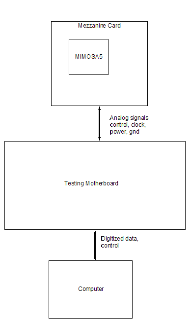
The MIMOSA5 detector is glue bonded to the mezzanine card and electrically attached with wire bonds.
The basic procedure is outlined below.
- Glue the MIMOSA5 detector to the bare mezzanine card with a dissolvable adhesive. We are using WaferGrip thin film adhesive. More information on this can be found here http://www.dynatex.com/products/WBS/wafergrip.html.
- Wire bond the detector to the mezzanine card pads. Place the wire bonds on the detector to one side of the pads. We have successfully removed and reattached up to 3 wire bonds per pad.
- Carefully mask the MIMOSA5 and solder the components to the mezzanine card.
- Characterize the detector.
- Remove the wire bonds.
- Use StripAid WaferGrip remover to remove the detectors from the mezzanine card. We have tested this and the stripper does not affect the electrical components.
- Thin the detector to the required thickness. This is a commercial process done at Aptek industries. http://www.aptekindustries.com/
- Glue the thinned detector to the original mezzanine card.
- Wire bond the detector to the mezzanine card pads.
- Re-characterize the detector.
We have tested the mechanical steps this process (except characterization) through with a red coded chip, and have been successful. Aptek is able to accommodate their grinding process to allow for the small residue of bond wire left on the silicon pads and deliver the chips ground to the correct thickness and with parallel sides.