LG 12/22/04
Testing Thinned MIMOSA 5 Chips
A first look
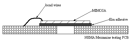
We intend to thin the MIMOSA detectors to a thickness of 50 μm for use in the HFT detector. While it is understood practice to thin Si chips to these thicknesses and still preserve functionality, we are thinning much larger pieces of Si and testing that the process works for us is a necessary precursor to building a prototype. In addition, we are intending to use a thin film adhesive that is rather soft to adhere the MIMOSA detectors to the cable and the process of bonding wires to the Si becomes harder.
The thinned 50 μm MIMOSA detectors were bonded to our standard mezzanine cards using 50 μm film adhesive. The MIMOSA detectors assemblies were then wire bonded to the PCB pads.
We received 2 MIMOSA wafers from LEPSI. The wafers were numbered B35739_09_G6 and B35739_L2_B6. Wafer # B35739_09_G6 was destroyed during the first attempt at thinning at the wafer scale. We then had Wafer # B35739_L2_B6 diced and half of the resulting individual MIMOSA detectors thinned.
The wafers were probe tested at LEPSI before they were shipped to us and each MIMOSA was given a color coding. As reported by Fabrice, the color coding was
RED = bad chip, no working sectors.
YELLOW = partially working chip. 1-3 bad sectors
GREEN = good chip, all sectors working.
The B35739_L2_B6 wafer had the following color coding;
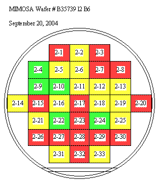
We tested bonded detectors from positions 2-12 and 2-13. These are yellow coded and thus we know only that the initial pre-thinned state was as indicated above.
Results:
2-12 (Mezzanine #5)
Sector 1 – DEAD
Sector 2 – Working but with some stuck columns
Sector 3 – Working but with a reduced response to light.
Sector 4 – Working but with a reduced response to light.
2-13 (Mezzanine #6)
Sector 1 – OK
Sector 2 – OK
Sector 3 – DEAD
Sector 4 – DEAD
Conclusions:
We have had success applying bonding wires to a 50 μm detector attached with 50 μm film adhesive. This bonding technique now appears to meet the requirements for out needs. The test for damage to the MIMOSA detectors during the thinning process is not definitive but very promising. Thinned detectors show the appropriate digital characteristics and all of the observed detector responses are consistent with their graded yellow status.
We will now proceed to thinning the rest of the detectors on wafer # B35739_L2_B6 and fabricating the prototype ladder.