LG 12/13/2004
Pixel Detector Prototype Cable Testing Results
We are examining the performance characteristics of the Pixel detector prototype cable. This is an active cable with a buffer and differential amplifier for each sector of 10 MIMOSA detectors. The circuit used is essentially the same as the one used currently in the testing mezzanine card.
This is all part of preparation for stage 1 and 2 of the Pixel Detector Prototype testing plan. The plan is documented here:
http://www.lbnl.leog.org/Pixel_Prototype_Testing.pdf
The circuit diagram for the one MIMOSA detector of the 10 on the cable is shown here:
http://www.lbnl.leog.org/SCHEMATIC1_PAGE5.pdf
We used the testing setup shown below:
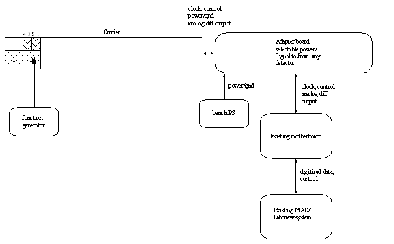
Figure 1
Test conditions for all tests:
- Va = 5 V, V- = -5 V, Vocm = 2.5 V, Vdig = GND
- Carrier position 2, Ch 3 input = GND
Testing for ambient noise level on Ch3. Ch 2 and Ch 4 have a 50 ohm to ground input.
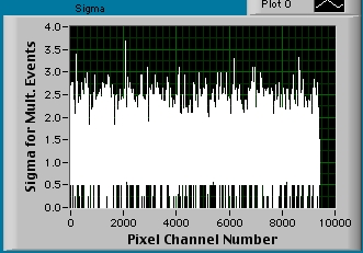
Figure 2
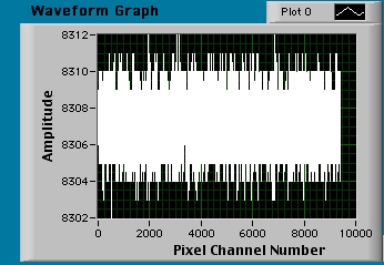
Figure 3
The RMS noise from the driver circuitry, cable and adapter board into the motherboard ADC is comparable to the noise found by grounding the motherboard ADC at the inputs.
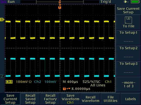
Testing for crosstalk on Ch3. Ch2 and Ch4 are driven with a 100 KHz, 500 mV square wave.
Ch 3.
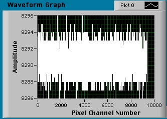
Figure 4
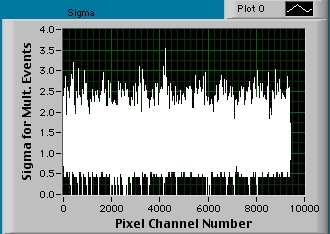
Figure 5
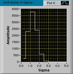
Figure 6
The RMS noise here is comparable to having no signal present in the adjacent channels.
Looking at ADC response through Ch 4. Ch2 and Ch 4 are driven with 500 mV square wave at 2.8 KHz
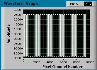
Figure 7
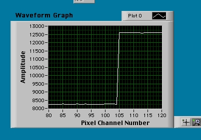
Figure 8
Looking at the small signal response. Ch 2 and Ch 4 are driven with 5 mV square wave at 2.8 KHz.
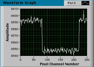
Figure 9
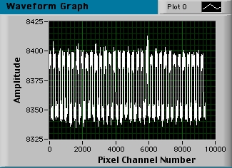
Figure 10
We also examined the signal shape response through the oscilloscope. Some scope pictures are posted below. Ch 1 is the waveform analog output measured through a probe at the output terminals of the adapter board. Ch 2 is the input pulse measured at the input to the buffer circuit on the cable.
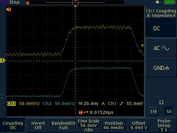
Note that the noise seem in the top (output) trace is not seen when testing small signals using the motherboard and ADC. This is likely some form of measurement noise associated with the scope/probe setup. The digitized 5 mV square wave in fig. 9 should be the basis of comparison.
In any case, the crosstalk seems quite low and not measurable in this setup. The signal response appears quite good. We will now move to adding MIMOSA detectors to a cable and loading the circuits to form a prototype ladder.